
Previous
Next


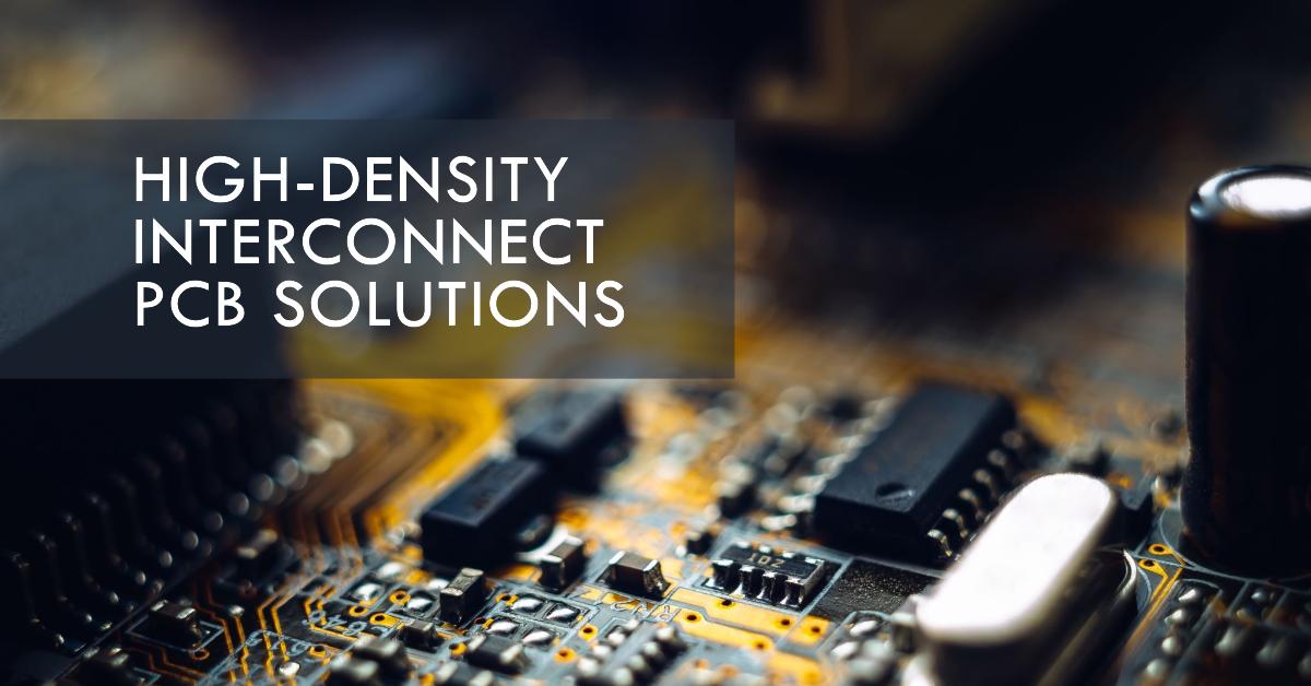
High-Density Interconnect (HDI) Manufacturer
Rush Flex PCB makes HDI or High-Density Interconnect PCBs. Such advanced printed circuit boards enable higher component density while providing more routing channels than traditional circuit boards allow. Thus, the advantage of HDI technology is, we can pack more components into a given area because of very fine tracks and spaces.
1
Step 1
keyboard_arrow_leftPrevious
Nextkeyboard_arrow_right
Why Use High-Density Interconnect (HDI) PCBs?
HDI technology is necessary for making smaller PCBs, or when the component pitch is very small. At Rush Flex PCB, we use HDI PCB design techniques when it is necessary to mount high component densities on limited board space. In fact, the component density decides the number of connections per square inch of the board.
For instance, if the connections of all test points and parts divided by the size of the board are below 120–130 pins per square inch, it is not necessary to use HDI, unless you are using a dense BGA that requires all connections. High-density PCBs offer several advantages including:
Lightweight and Compact Sizing
The higher wiring density per unit area of the HDI PCB allows for mounting more components on a tiny board. Consequently, it typically leads to a smaller assembly useful for making devices like tiny, multifunctional medical devices, thin, powerful smartphones, and wearables.
Improved Signal Integrity
Via-in-pad and blind vias allow placing components closer to each other, thereby reducing the signal transmission path. Hence, this arrangement reduces or even eliminates the occurrence of signal reflections, resulting in improved signal quality throughout the circuit. Moreover, devices like phones and wearables operate with zero glitches because of the improved signal integrity.
Increase in Design Flexibility
Laser-drilled microvias provide high-density interlayer connections, facilitating routing paths for densely packed components with high pin counts, like BGAs.
Better Reliability and Performance
It is possible to mount several small active components to form a tight circuit on a small area, thereby increasing the board’s overall performance. Improved signal integrity helps to enhance reliability.
Supports Miniaturization of Electronics
As we can pack more functionality into a compact area of the PCB, HDI technology facilitates the miniaturization of end products such as wearables and mobile devices.
Potential Layer Count Reduction
With the efficient utilization of available routing area per layer, HDI technology potentially achieves the same component placement and circuit connectivity with fewer PCB layers compared to conventional designs. Furthermore, this also helps to lower fabrication costs.
Key Features of Rush Flex PCB HDI PCBs
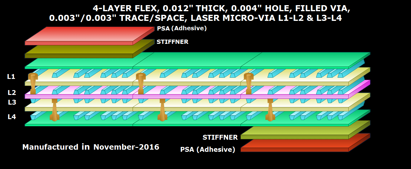
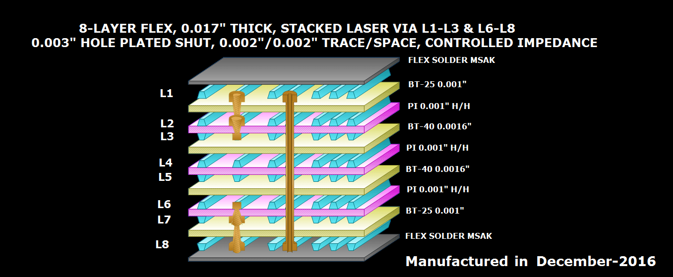
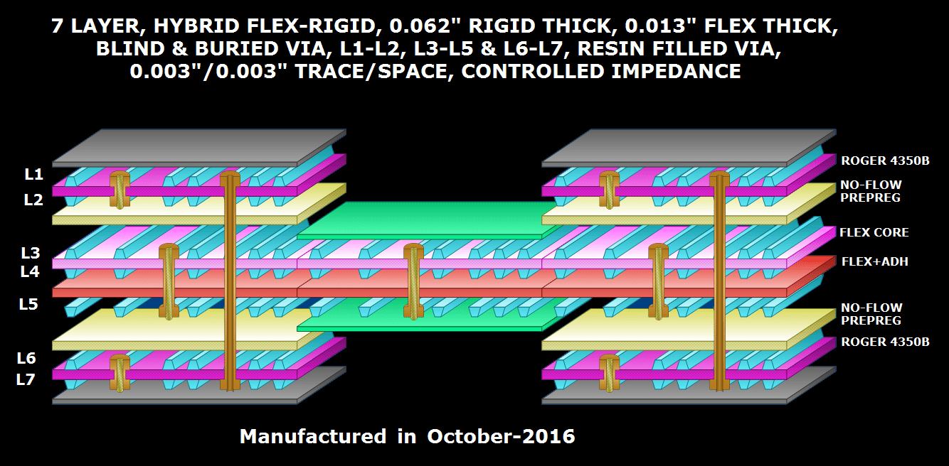
SBU or Sequential Build-Up: Firstly, this is a term referring to the process of building a multilayer PCB. Essentially, we build up the PCB layer-by-layer using multiple subcomponents of copper sheets and thin insulating laminate materials.
Microvias: Secondly, these are laser-drilled, plated blind hole structures with a maximum aspect ratio of 1:1 between their depth and hole diameter. The depth generally does not exceed 9.84 mils (0.25 mm) from the land foil to the target pad or plane.
Blind Vias: Thirdly, these are plated holes interconnecting an outermost layer to any inner layer, but not going through the entire PCB thickness or structure.
Buried Vias: These are plated holes interconnecting one or more inner layers without exiting to any of the outermost layers, and therefore, being invisible from the outside.
Via-in-Pad: Finally, these are plated holes positioned in the copper landing pad of a component. We typically fill them with non-conductive epoxy, cap them, and then plate them over.
Different Types of HDI PCBs from Rush Flex PCB
We make six types of HDI PCBs, including:
Type I
These HDI PCBs have only a single layer of blind and through-hole vias on one or both sides of the core or substrate material. There are no buried vias.
Type II
These multilayer HDI PCBs feature stacked microvias and through-hole vias and may include some buried vias filled with non-conductive or conductive paste. Moreover, the buried vias may also be fully or partially filled with dielectric material during the lamination process.
Type III
These multilayer HDI PCBs feature stacked microvias in two or more layers along with through-holes and buried vias. Similar to the Type II PCBs, all buried vias may be prefilled with non-conductive or conductive paste. Further, they may also be fully or partially filled with dielectric material during the lamination process.
Type IV
These HDI PCBs are made of a passive substrate without any electrical connections. Thus, this core typically provides CTE, shielding, or thermal functions.
Type V
These multilayer HDI PCBs are coreless. They contain an even number of layers that have been laminated together while making interconnections between the odd and even layers. Thus, as this is a single lamination process, it does not involve SBU.
3+N+3
In this type of stack-up, we offer six signal-routing layers, three on the top and three at the bottom layers of the board. Moreover, in between these layers are N number of sequential build-up layers. The board provides routing on six outer layers.
Any Layer HDI
Finally, this is our most advanced HDI type, where we provide high-density interconnects on any layers including the core layers, offering maximum routing flexibility.
Our HDI PCB Manufacturing Process and Technologies
Undoubtedly, fabricating high-quality HDI printed circuit boards requires specialized materials and advanced manufacturing processes, including:
Thin Dielectric Materials
We use a very thin base dielectric material of 1 mil (25 microns) for the core layers. We fabricate sequential build-up layers using thin dielectric laminates. Therefore, this allows us to achieve the geometries necessary for fine traces and spacing.
Laser Drilling Technology
We typically use laser drilling to make microvias in our HDI boards. These are small via holes of high-precision location with diameters of about 50 microns or less. Additionally, we also use laser drilling for stacked and staggered microvias to optimize the routing.
Sequential Lamination Process
Unlike our standard lamination process, we use a sequential lamination process for our HDI boards. Here, we laminate the core, build up dielectric materials, and the copper foils together, one layer at a time. So, this process allows us to achieve overall board thicknesses as low as 0.4 mm for an HDI board with a 10+ layer count.
Microvias with Copper Filling
We plate the microvias with copper using electrolytic and electroless plating processes. Accordingly, this allows us to create continuous conductive pathways between the layers that the vias interconnect.
Routing and Laser Imaging
We use tight tolerance laser imaging to achieve very fine line patterns during the routing and imaging process. ence, we achieve greater precision during the sequential build-up process, minimizing registration issues.
Why Choose Rush Flex PCB for HDI PCB Needs?
Rush Flex PCB is a single-window hub for PCB procurement. We do not follow the old, complicated, and slow way of manufacturing PCBs that everyone is used to. We organize the complete production process of the High-Density Interconnect (HDI) PCB for you, allowing you to focus your energy and resources on product development. Additionally, we collaborate with you to optimize your HDI design or match your finished designs with our expertise in manufacturing. Subsequently, we guarantee that you will receive your high-quality PCBs on time, every time.
Our HDI PCB capabilities include:
- High layer count designs — 6+ layers
- Track width and line spacing as low as 2 milmils
- Precision laser-drilled microvias with 5 mil diameters
- Core dielectric layers as thin as 1 mil
- Engineering collaboration for cycle time optimization
- 100% electrical testing for every bare HDI board
- Quick-turn engineering prototypes with fast iterations
- Large, medium, and low-volume production.
Thus, you can contact us via e-mail or by phone to discuss your next High-Density Interconnect (HDI) project. Further, you can also use our online inquiry form to get an instant HDI PCB quote. We have a team of engineers ready to assist you and deliver advanced solutions to your complex HDI designs using cutting-edge HDI expertise tailored to your requirements.
Frequently Asked Questions
The construction of HDI PCBs allows for very high routing and component density as compared to regular PCBs. For this, the HDI PCBs use very thin dielectric layers, small diameter microvias, finer trace widths and spacings, and higher layer counts for PCBs with 8+ layers.
Microvias are like normal vias, but much smaller, and they interconnect traces between layers on HDI PCBs. They typically have diameters less than 150 microns. We drill microvias using lasers and then plate them with copper to create a conductive path between layers.
We use four types of layer stackup configurations for our HDI PCBs. Three of them are — 1+N+1, 2+N+2, 3+N+3 — all having N number of sequential buildup layers between the outer signal routing layers. The fourth type is Any Layer HDI, which allows interconnections on any layer.
Yes, we can accommodate plated through holes in our HDI PCBs and these can take in through-hole-type components. For this, we provide clearance holes in the high-density buildup layers to allow the barrels of the PTH to pass through without any obstructions.
To achieve fine line patterns during the routing and imaging process, we use tight tolerance laser imaging. We also use a sequential buildup process to minimize registration issues and thereby achieve greater precision.